Screenshot Bark Scanning Filter FPD file
Motivation
t.b.d.
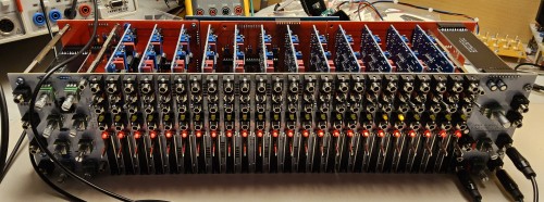
- Completely analog
- Up to 24 filters
- Modular
- t.b.d.
- ...
t.b.d.
Bark Scanning Filter PCB's |
|
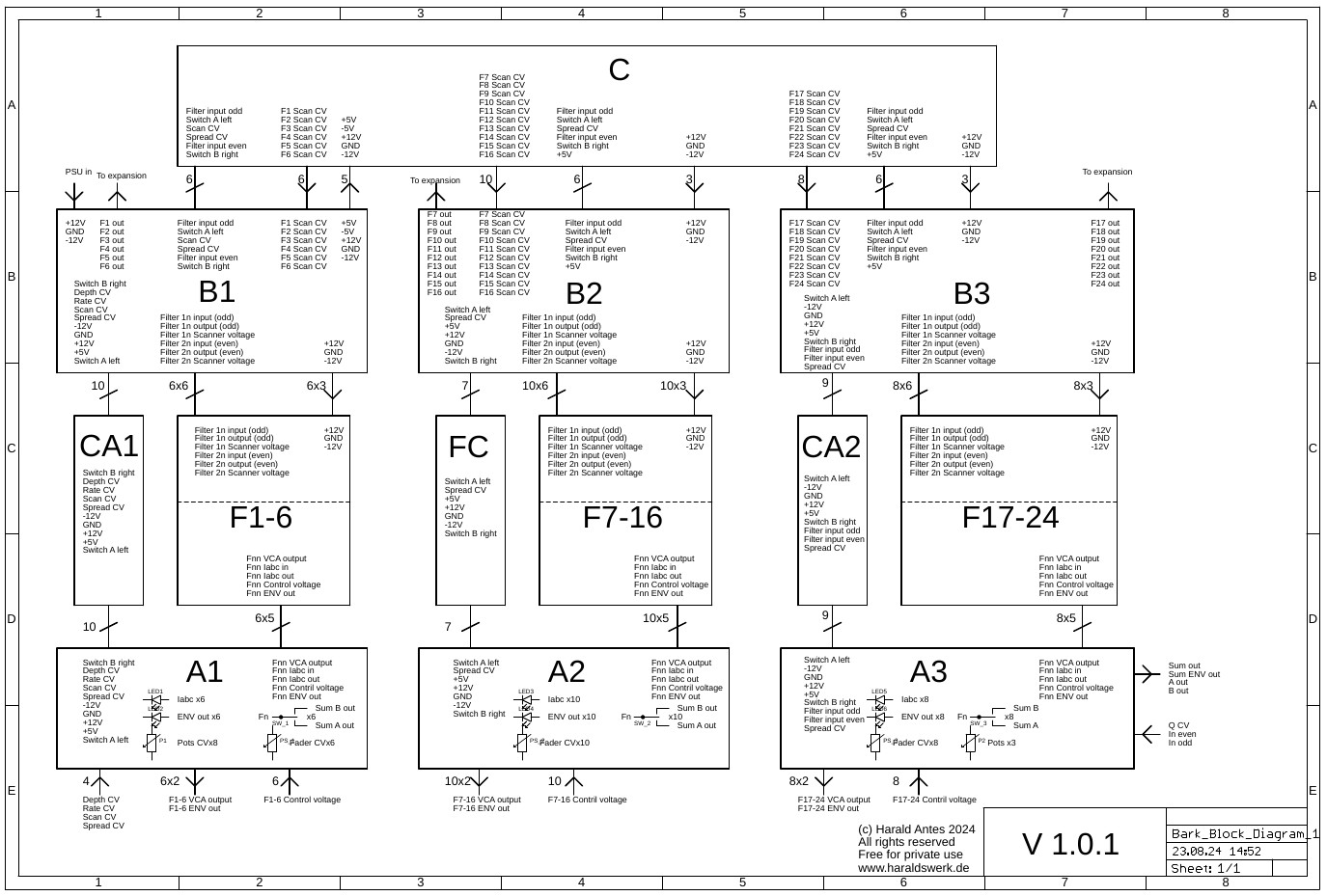
PCB-A1, CV inputs, IO for filters 1-6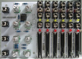
PCB-A1, CV inputs, IO for filters 1-6Top |
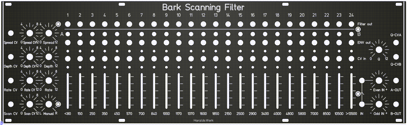
Current state: PublishedThis PCB holds the control voltage inputs for spread, scanning depth, LFO rate and scan CV with the dedicated attenuators and the manual controls. As well as the in- and outputs for the Bark filters 1-6 and the manual control for the dedicated VCA's. For understanding how everything works together please have a look at the block diagram on the project page. |
PCB-A2, CV inputs, IO for filters 1-6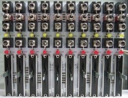
PCB-A2, CV inputs, IO for filters 7-17Top |
Current state: PublishedThis PCB holds the single outputs for the Bark filters 7-16, the envelope outs, the control voltage ins and the manual fader controls for the dedicated VCA's. The control voltages for the VCA's are signaled with LED, as well as envelope outputs for each channel. For understanding how everything works together please have a look at the block diagram on the project page. |
PCB-A2, CV inputs, IO for filters 1-6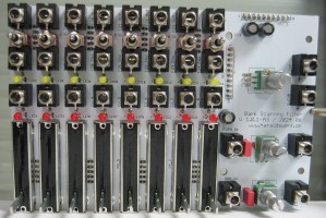
PCB-A3, Audio in- and outputs, CV inputs, IO for filters 17-24Top |
Current state: PublishedThis PCB holds the audio inputs for the odd and even filters. The odd input is normaled to the even input. Both inputs have attenuverters. Those makes for interesting sonic effects when the feedback is engaged. The outputs A and B sums the individual outs from the filters according to the position of the select switches (A, B, off). The Q potentiometer adjust the amount of feedback used. The feedback is voltage controllable. The PCB holds the single outputs for the Bark filters 17-24, the envelope outs, the control voltage ins and the manual fader controls for the dedicated VCA's as well. The control voltages for the VCA's are signaled with LED, as well as envelope outputs for each channel. For understanding how everything works together please have a look at the block diagram on the project page. |
PCB-LF, low pass / band pass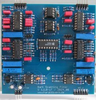
PCB-LF, low pass / 2 band passTop |
Current state: PublishedThis PCB holds the first and second Bark filter. Filter one is a low pass with 80Hz corner frequency, filter two is the first band pass with 150Hz center frequency. It holds the associated VCA's and the associated precision full wave rectifiers as well. For understanding how everything works together please have a look at the block diagram on the project page. |
PCB-FF, band pass / band pass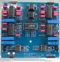
PCB-FF, band pass / band passTop |
Current state: PublishedThis PCB holds the band pass filters for Bark scanning filter. The filters 2-23. You need ten of them each with two filters. It holds the associated VCA's and the associated precision full wave rectifiers as well. For understanding how everything works together please have a look at the block diagram on the project page. |
PCB-FH, band pass / high pass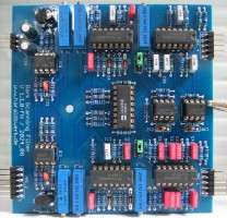
PCB-FH, band pass / high passTop |
Current state: PublishedThis PCB holds the twenty third and twenty fourth Bark filter. The last band pass with 10500Hz center frequency and the high pass with 13500Hz cut off frequency. It holds the associated VCA's and the associated precision full wave rectifiers as well. For understanding how everything works together please have a look at the block diagram on the project page. |
PCB-B1, scanning LFO, voltage reference, PSU in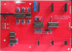
PCB-B1, scanning LFO, voltage reference, PSU inTop |
Current state: PublishedThis PCB holds the scanning LFO and the output buffers for the optional/additional filter out 1-6. As well as the power supply input and the 5V voltage reference. For understanding how everything works together please have a look at the block diagram on the project page. |
PCB-B2, optional/additional output buffers for channels 7-17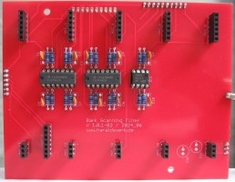
PCB-B2, additional/optional filter outsTop |
Current state: PublishedThis PCB on the back of the middle section holds output buffers for the optional/additional filter outs 7-17. It carries all the necessary signals and control voltages from the left to the right building block and back. And it holds the middle section together. For understanding how everything works together please have a look at the block diagram on the project page. |
PCB-B3, optional/additional output buffers for channels 18-24
PCB-B3, additional/optional filter outsTop |
Current state: PublishedThis PCB on the back of the right section holds output buffers for the optional/additional filter outs 18-24. It carries all the necessary signals and control voltages from the right to the middle building block and back. And it holds the right section together. For understanding how everything works together please have a look at the block diagram on the project page. |
PCB-C, Scanner unit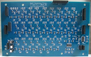
PCB-C, Scanner unitTop |
Current state: PublishedThis PCB builds the heart of the Bark Scanning Filter. The scanner unit. The PCB connects all the necessary signals and control voltages between left, right and middle building block. And it holds all building blocks mechanical together. For understanding how everything works together please have a look at the block diagram on the project page. |
Pre Fader Out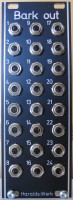
Pre Fader OutTop |
Current state: PublishedThis is an additional module that gives you direct access to the individual filter outs, pre fader, for each band. The module is passiv. All circuitry is on the main module. |