Motivation
My original Elektor Formant VCA used two 3080 in series. In most cases only one is used and the second only adds to noise and distortion. This VCA is AC coupled only. The THD in the Elektor Formant VCA is about 1% and the noise to voltage ratio is not that good either. Time to look for a replacement. I wanted a decent DC coupled audio VCA to process audio as well as control voltages. And easy available parts (2014/08). I tried different architectures and then decided to separate audio and DC VCA. With specialized VCA it is easier to reach both goals. I made my own implementation of the Sims-VCA introduced by Mike Sims in the EDN Magazine January 1995. With this architecture it is possible to achieve THD of 0,02%.
Unfortunately i can not confirm the statement from Mike Sims that trimming the circuit for minimum THD achieves minimum control voltage feedthrough. Trimming for minimum THD causes an constant DC bias at the output. I have had to add a output capacitor to avoid the bias at the output. And you need test equipment to measure the THD for correct trimming. If you can not measure THD better build my DC-VCA . You can achieve 0,2 % THD here. Still good.
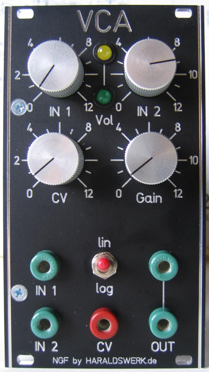
Specs and features:
- AC coupled 0,02% THD
- lin and log response
- CV 0..+5V
- 5Vpp in- and output
- simple Level indicator
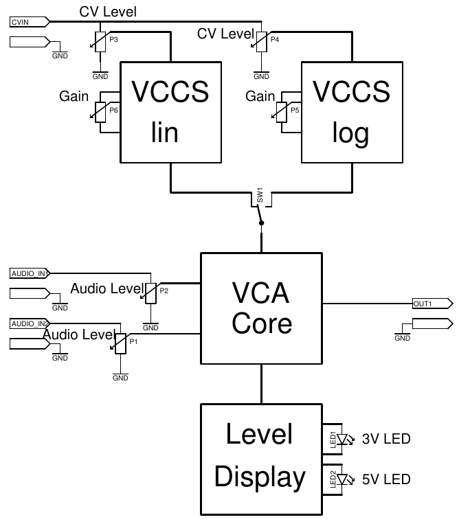
- Block diagram
- Schematic
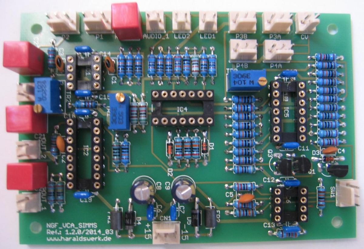
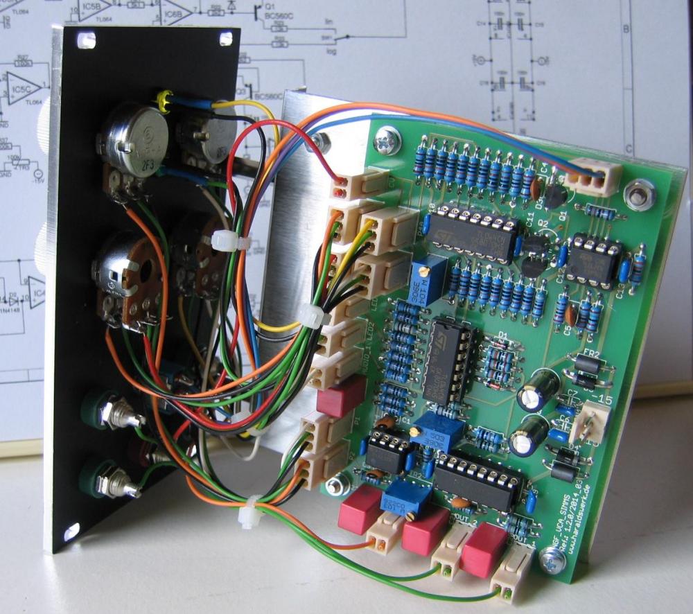
- Pictures
Simulation
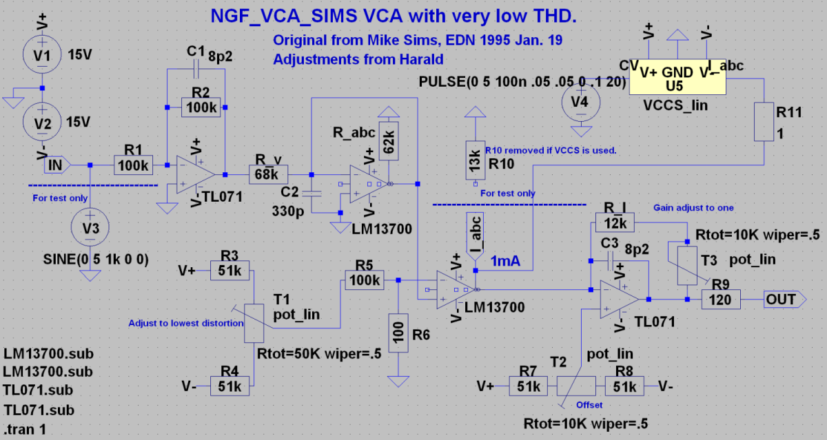
NGF VCA Sims simulation
Only the audio path is shown here.For CV VCCS lin is used with a triangle curve.
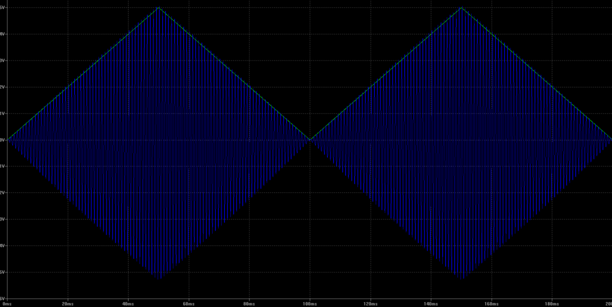
NGF VCA Sims adio output
As you can see the audio output (blue lines) follows the CV curve (green line) very well.
Implementation
Schematic
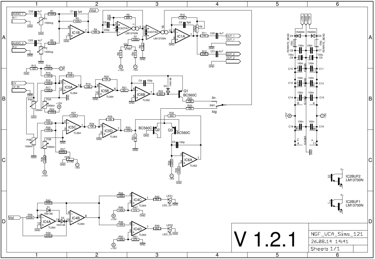
NGF VCA Sims schematic
Description
There are four blocks in the Schematic. From the top: Audio path, VCCS lin, VCCS log, Level display. The audio path starts with an voltage adder. You can add more inputs here if needed and adjust the input level. IC2OTA1's negative-feedback configuration forces the current from IC2OTA1's pin 5 to equal the ac-input current through R4 . IC2OTA1's pin 5 also connects to IC2OTA2's pin 14, causing a virtually identical current to flow from IC2OTA2 's pin 12. IC1A converts this current to an output voltage. The output voltage is adjusted with TR2 for different Gm off OTA's. The implementation differs in some details from the simulation.
For more details of the VCCS lin look here.
For more details of the VCCS log look here.
For more details of the level indicator look here.
Calibration
- Insert 5Vpp sinus signal to one off the inputs. Set pot to max. Choose linear response. Set Gain to max. Adjust TR2 for the output to match the input signal.
- Adjust TR1 for lowest THD
- Choose log response. Set gain to zero. Adjust TR3 for zero signal bleedthrough.
Special parts
None. You might want to select the LM13700 for best performance. They differ quite a lot from chip to chip and manufacturer.