Motivation
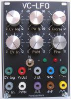
This is the flat version of my VC LFO. I've build this flat version to minimize the depth of the module and avoid the wiring for the potentiometers. A VC LFO with multiple synced output waveforms is a very useful and versatile module. You can't have enough of them. They can add a lot to sounds making them more animated. This one provides triangle, ramp up, ramp down pulse. square and sine wave output (-5V to +5V). The frequency range is easily adjusted to your needs from some minute per cycle up to 40Hz. I started with the VC LFO design form Ray Wilson MFOS but changed the exponentiator and pulse adjust schematic completely. I have added a range switch and a linear FM input as well.
Specs and features
- Synced triangle, ramp up, ramp down, pulse, square and sine wave output
- Output -5V to +5V
- log and lin CV input
- Temperature compensated
- Voltage controlled pulse width
- Range switch
- Coarse and fine frequency setting
- Runs on +/-15V and +/-12V
- Power consumption below 10mA each rail
Implementation
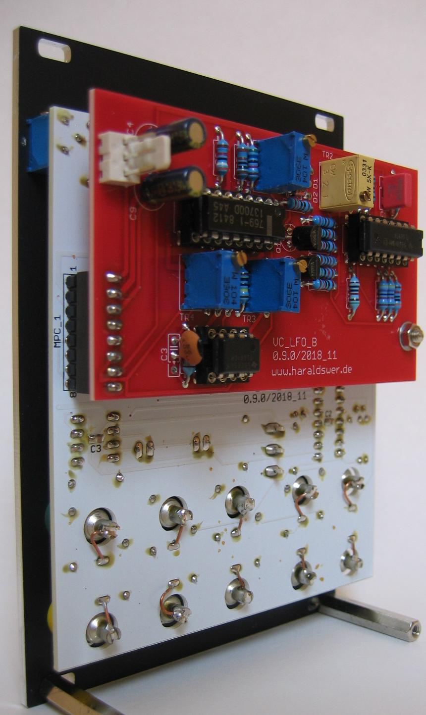
Schematic

VC LFO front PCB schematic
 >
>
VC LFO back PCB schematic
Description:
IC1 and associated components comprise a linear voltage to log current converter. IC1A sums the control voltages. IC1B provides the temp compensation realized with KTY81-110. TR3 adjusts the V/Oct characteristic. Q1 and Q2 forms the log converter with IC1D as constant current source. IC1C scales the control voltage for the linear FM input. The transconductance of IC1OTA1 controls the frequency of the oscillator. IC2C, C1 and associated components comprise an integrator. When current flows into IC1OTA1 output the integrator ramps up, when current flows out of IC1OTA1 the integrator ramps down. When the integrators output goes above the threshold of comparator IC2D its output goes high. The output of IC2D is fed to the non-inverting input of IC1OTA1 OTA through D1, D2, R1, R2 and TR1. TR1 balances the current flowing during the high and low periods of IC2D. With TR1 you can adjust the symmetry of the triangle. While IC2Ds output is high current flows out of IC1OTA1 OTA and the integrator ramps down until the voltage at the input of IC2D goes low enough to overcome the hysteresis provided by R13 and its output goes low. When this happens the comparator starts to ramp up again and thus we have a triangle wave at the output of IC2C. The bias of the comparator IC2D is controlled by the current generated by the linear voltage to log current convertor. This controls the current that flows in and out of IC1OTA1 and thus the frequency of the oscillator.
The sawtooth is created by mixing portions of the original triangle wave and an inverted version of the triangle wave. N-FETs Q1 and Q1 are used as analog switches.
To be continued
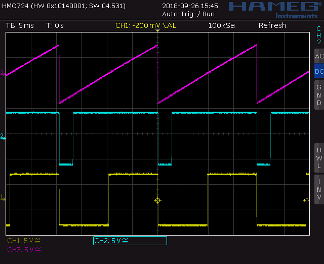
VC LFO screenshot: Waveforms ramp up, pulse, square
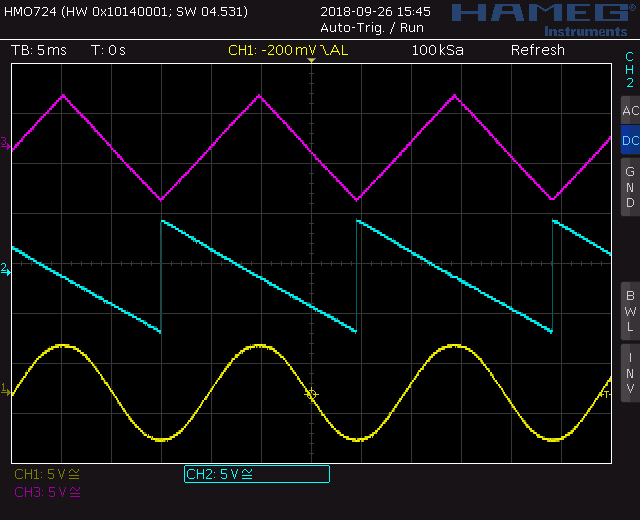
VC LFO screenshot: Waveforms triangle, ramp down, sine
Top
Calibration
- Start with the triangle symmetry. Adjust symmetry with TR1
- Ramp up/down. Look at the ramp output. Adjust TR2 so that the ramp wave is continuous. If TR2 does not allow you completely null the step (you can't go low enough or you can't go high enough) then adjust the value of R19 a few K up or down until TR2 gives you the range you need
- Pulse symmetry. Set the PW pot P6 to the center point. Adjust TR4 for the pulse output symmetry.
- Sine adjust. You have to experiment here a bit until you are satisfied. Adjust TR4 for the sine volume and TR3 for the sine shape. They are not independent. Trial and error helps. If you are not satisfied with the outcome you can experiment with changing R21, R22 and R24.
- log adjust. Set TR3 so that a 1V voltage change at the V/Oct input causes a change og 17.3mV at the basis of Q1. Don't expect a close V/Oct characteristic. But it is not bad either.
- Initial frequency adjust. Set SW1 to hi. Adjust TR1 to about 10Hz. Set SW1 to lo. Adjust TR2 to 1Hz. This is only a starting point. You can set the initial frequency where ever you want. Hint: Build multiple LFO. You will need them.
Special parts
None
Download
VC LFO documentation downloadVC LFO Gerber files back PCB download
VC LFO Gerber files front PCB download
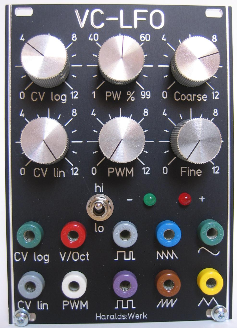
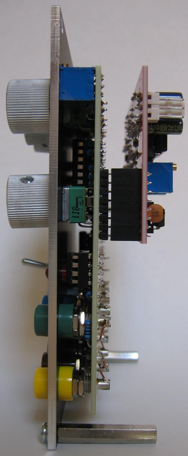
VC LFO: Front view
VC LFO: Back view