Motivation
This is the flat Version of my NGF DC VCA. I wanted a decent DC coupled audio VCA to process audio as well as control voltages. And easy available parts (2018/07). I tried different architectures and then decided to separate audio and DC VCA. With specialized VCA it is easier to reach the goal. For control voltage processing I implemented a VCA with active control voltage feedthrough compensation. For lowest control voltage feedthrough you have to use low Iabc as well. So the audio performance is not as good as in my NGF VCA Sims. THD is about 0,2% with selected LM13700. Still not bad and sufficient for DC usage. For DC processing you want to keep the feedthrough and bias of the control input as low as possible. There can be 500mV or more offset depending on the control voltage (I_abc) and it doesn't vary linearly. There's a big bump in offset right in the middle of CV range. First thing to do is to lower I_abc to around 250uA. This helps for DC performance but degrades AC performance. The main idea is to use the second OTA of the 13700 to compensate for the CV feedthrough. Both OTA in the 13700 are on the same chip and behaves the same. So I inverted the output of the second OTA and added it to the signal path. You still have to select the LM13700 for best performance.
Specs and features:
- DC coupled
- Active CV feedthrough compensation
- Linear response
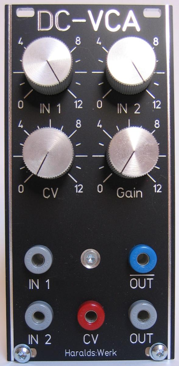
- CV 0..+5V
- 5Vpp in- and output
- Positive and negative output
- Runs on +/-15V and +/-12V
- Power consumption below 20mA each rail
- Schematic
- Documentation for download
- Pictures
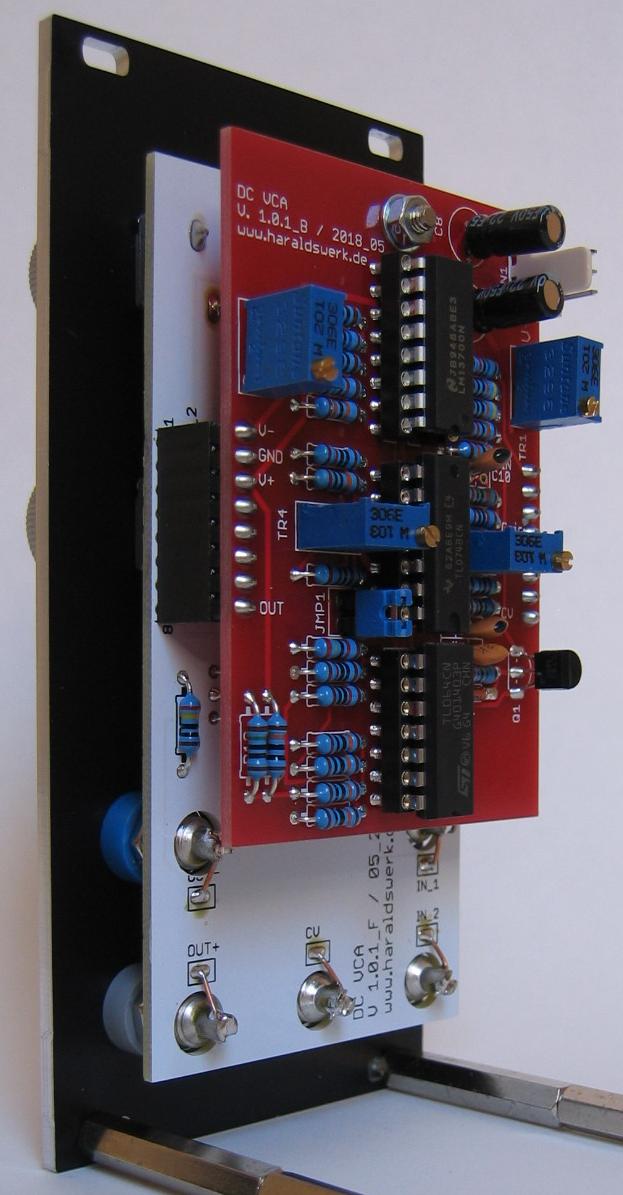
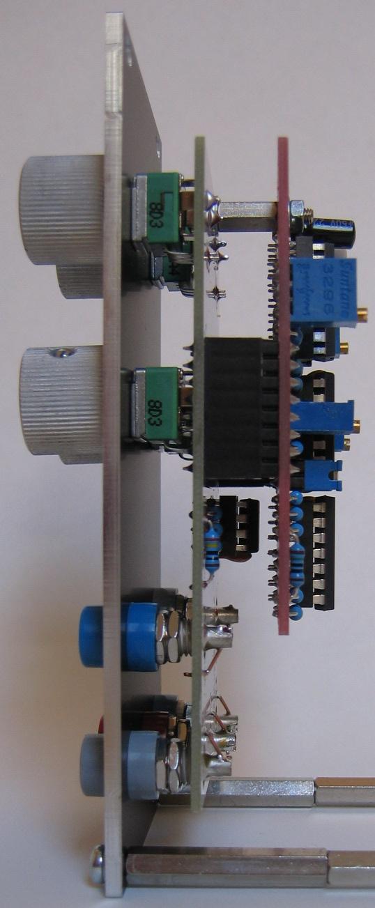
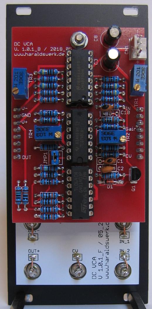
Implementation
Schematic
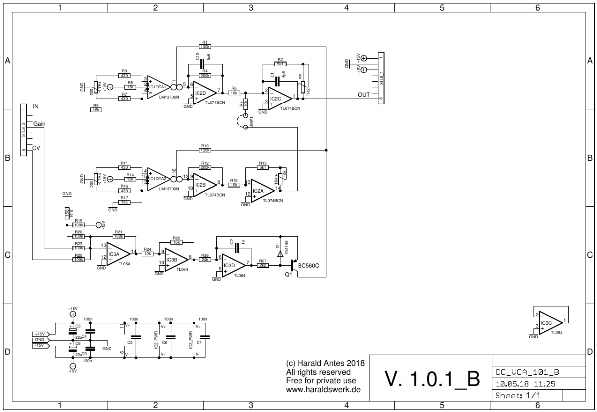
DC VCA flat schematic back PCB
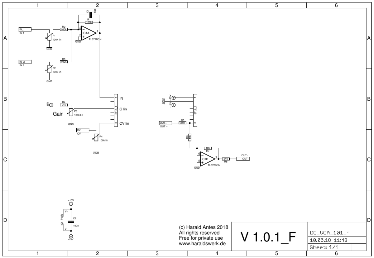
DC VCA flat schematic front PCB
Description:
On the top is a plain forward implementation for an VCA. Next row is the same VCA with input set to ground and output inverted. The inverted output of the second VCA is added to the output of the first one to compensate for the CV feedthrough. The output voltage is adjusted with TR2/TR4 for different Gm off OTA's.
Calibration
- DC Path: Ground input (Both pots to GND). Set gain pot to max. Jumper JMP1 open. Measure output voltage. Adjust TR1 for zero voltage.
- Compensation Path: Set gain pot to max. Jumper JMP1 open. Measure voltage at pin14 from IC2A . Adjust TR3 for zero voltage.
- Compensation adjust: Ground input (Both Pots to GND). Measure output voltage. Set gain pot to max output voltage (around center point). Close Jumper JMP1. Adjust TR4 to zero output
- Apply input voltage signal 5Vpp. Set input pot to max. Set gain pot to max. Set TR2 to equal input and output (Use oscilloscope.).
Special parts
- None. You might want to select the LM13700 for best performance. They differ quite a lot from chip to chip.