Motivation
My original Elektor Formant VCA used two 3080 in series. In most cases only one is used and the second only adds to the noise and distortion. He is AC coupled only. The THD is about 1% and the noise to voltage ratio is not that good either. Time to look for a replacement. I wanted a decent DC coupled audio VCA to process audio as well as control voltages. And easy available parts (2014/08). I tried different architectures and then decided to separate audio and DC VCA. With specialized VCA it is easier to reach the goal. For control voltage processing I implemented a VCA with active control voltage feedthrough compensation.
For lowest control voltage feedthrough you have to use low I_abc as well. So the audio performance is not as good as in my NGF VCA Sims. THD is about 0,2% with selected LM13700. Still good. If you can only build one VCA i recommend building this one. You can use it for audio as well and it is still better than the 3080.
For DC processing you want to keep the feedthrough and bias of the control input as low as possible. There can be 500mV or more offset depending on the control voltage (I_abc) and it doesn't vary linearly. There's a big bump in offset right in the middle of CV range. First thing to do is to lower I_abc to around 250uA. This helps for DC performance but degrades AC performance. The main idea is to use the second OTA of the 13700 to compensate for the feedthrough. Both OTA in the 13700 are on the same chip and behaves the same. So i inverted the output of the second OTA and added it to the signal path.
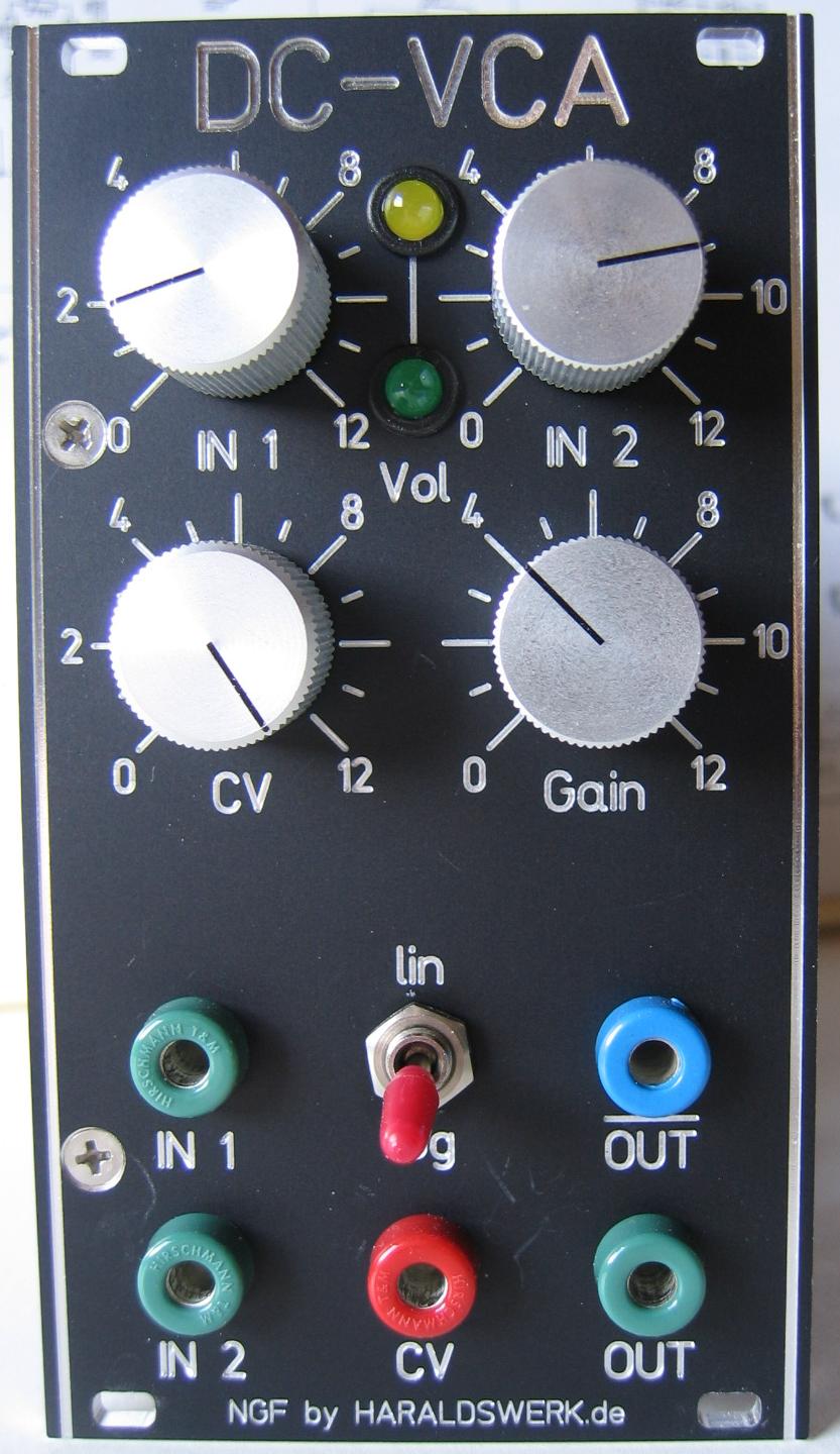
Specs and features:
- DC coupled 0,2% THD
- Active CV feedthrough compensation
- Lin and log response
- Control Voltage 0..+5V
- 5Vpp in- and output
- simple Level indicator
- PSU +/-15V
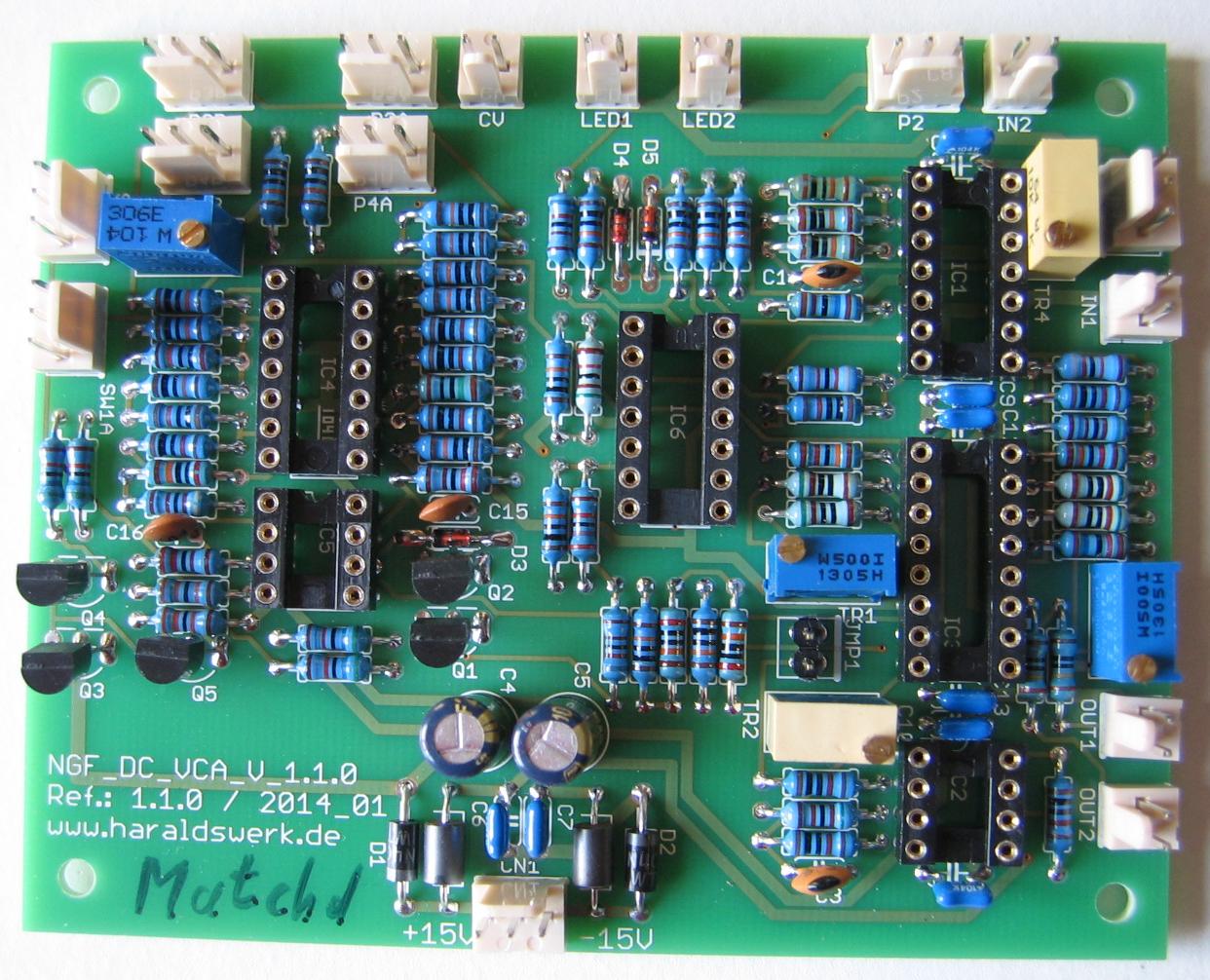
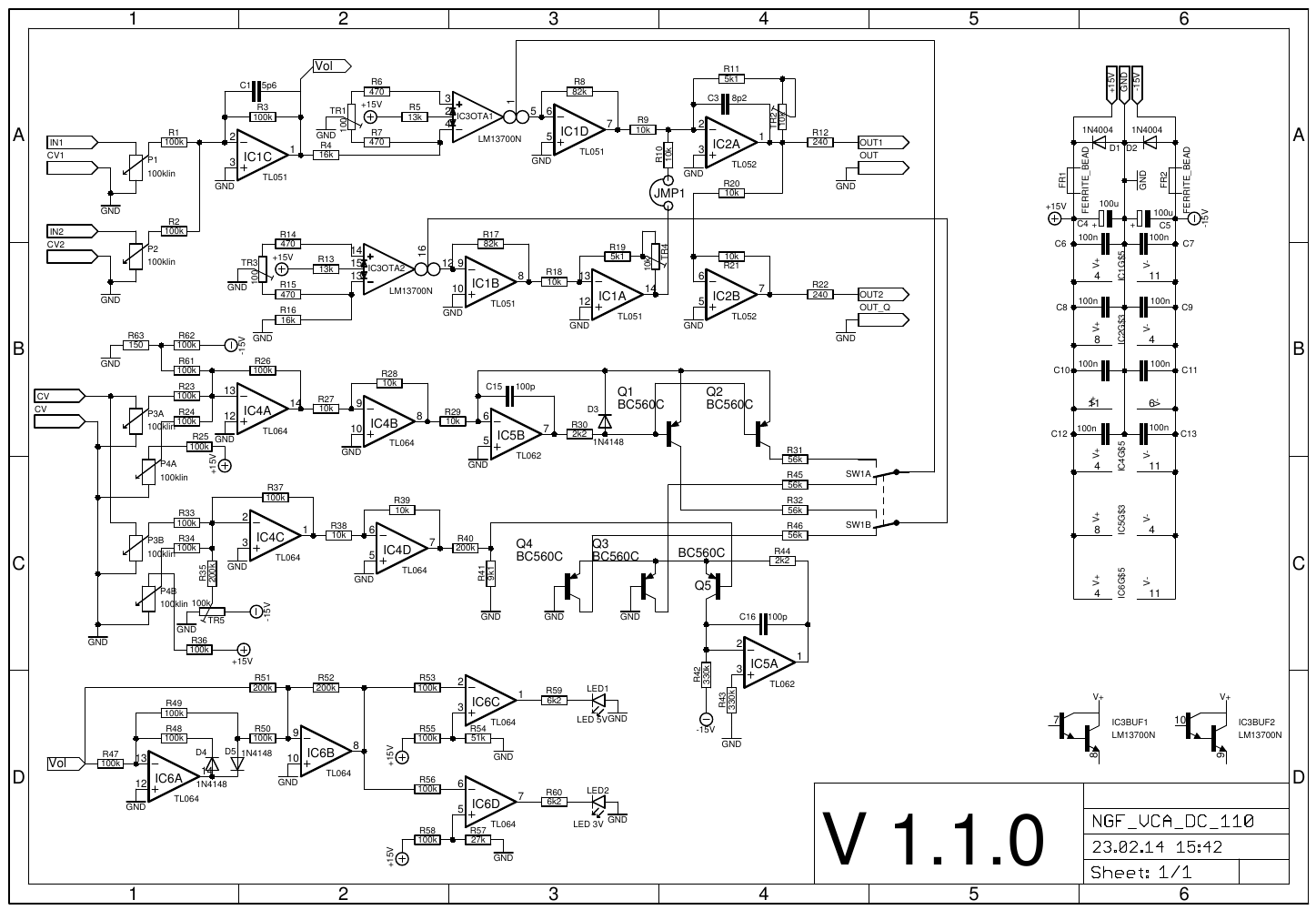
- Schematic
Simulation
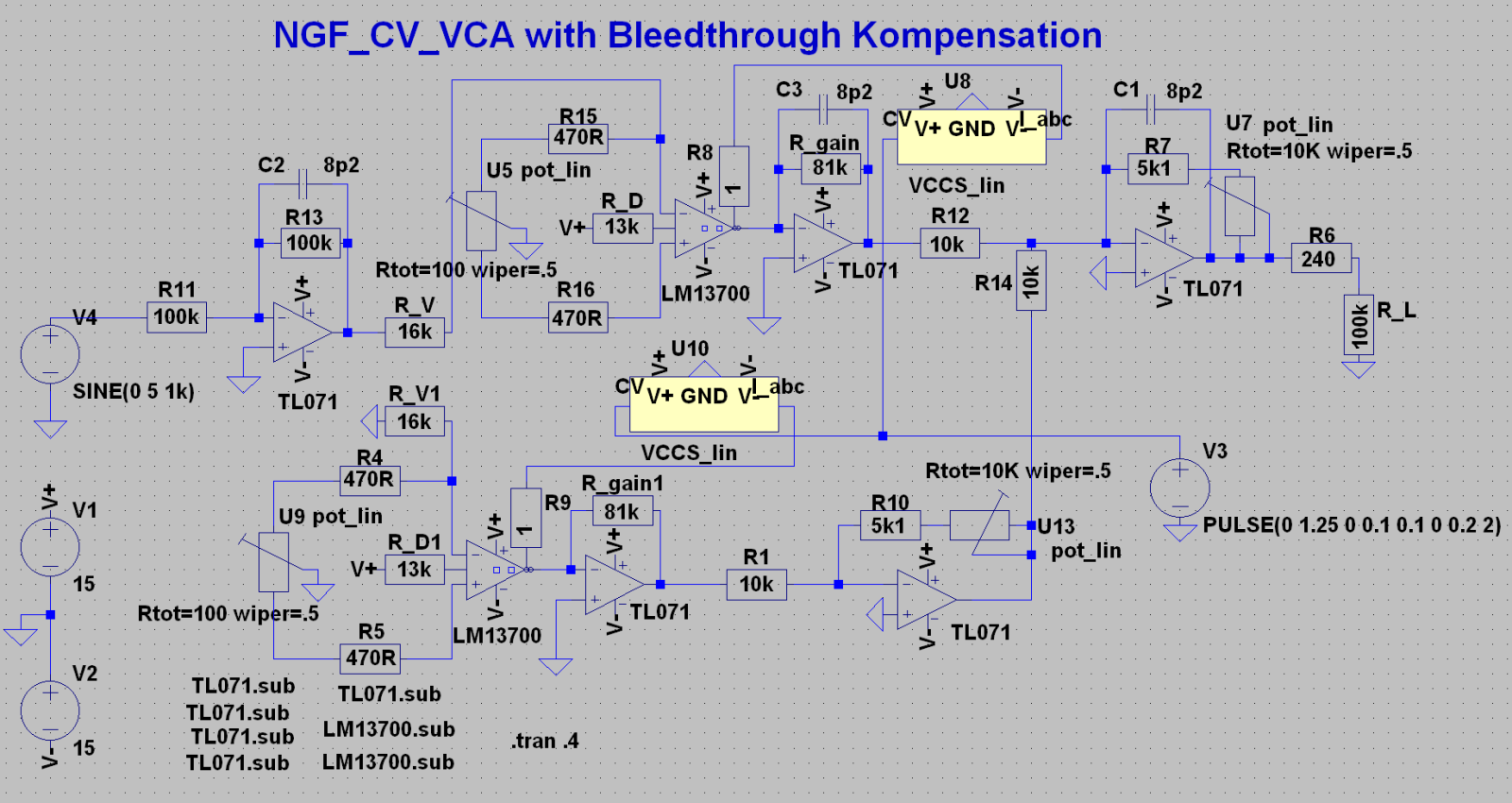
Only the DC/audio path with CV feedthrough compensation is shown here. For CV, VCCS lin is used with a triangle curve.
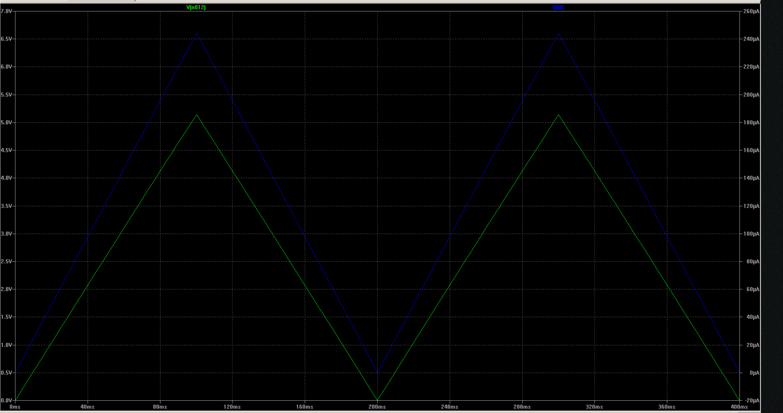
As you can see the DC/audio output (green line) follows the I_abc curve (blue line) very well.
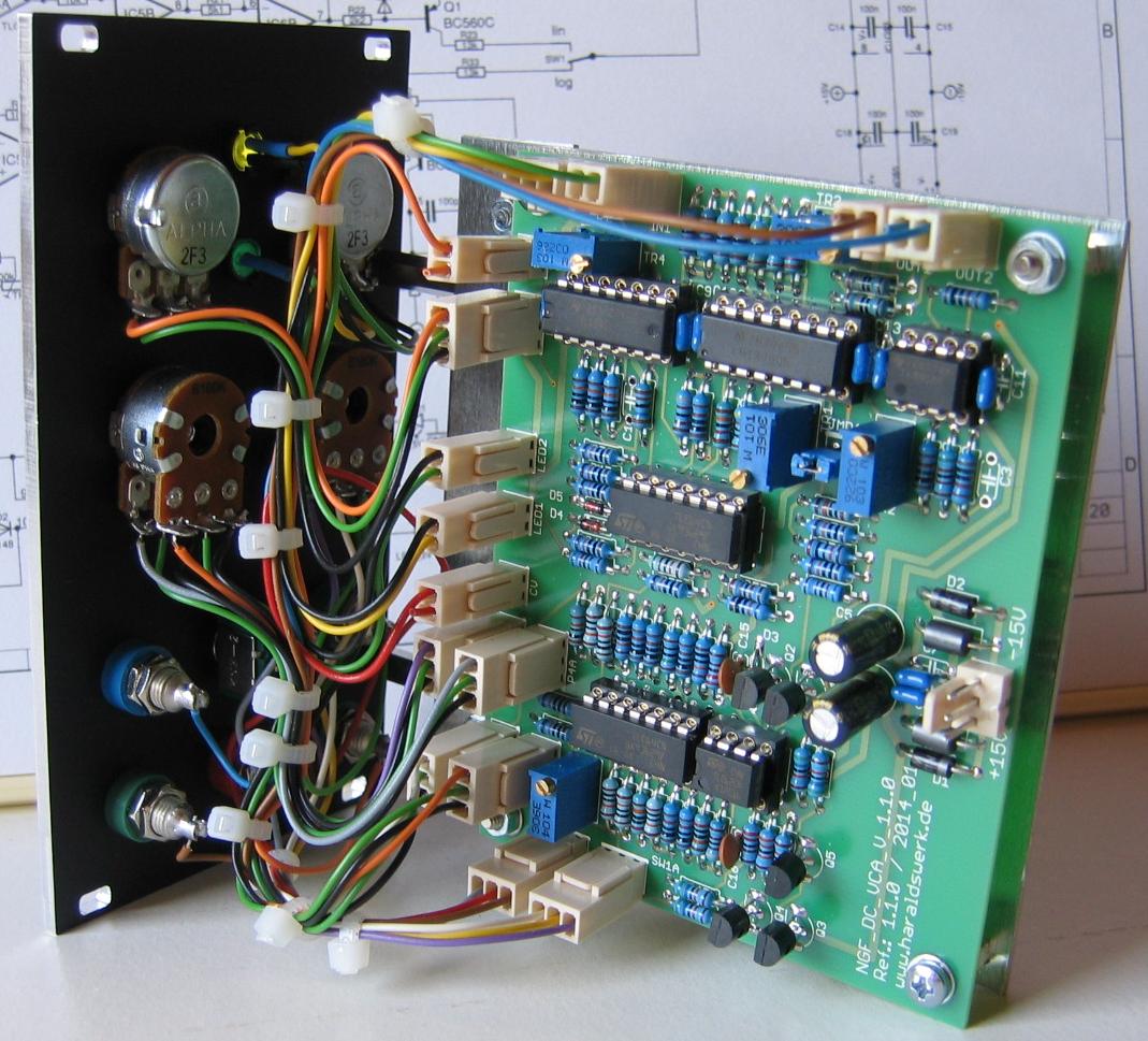
Implementation
Schematic
Description
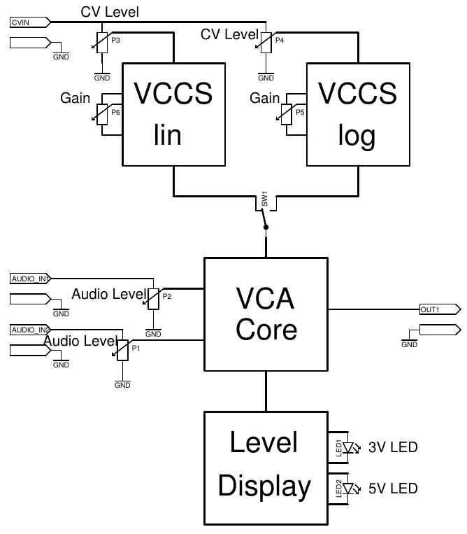
There are four blocks in the Schematic. From the top: DC or Audio path with CV feedthrough compensation, VCCS lin mult, VCCS log mult, Level display. On the top is a plain forward implementation for an VCA. Next row is the same VCA with input set to ground and output inverted. The inverted output of the second VCA is added to the output of the first one to compensate for the CV feedthrough. The output voltage is adjusted with TR2/TR4 for different Gm off OTA's. The implementation differs in some details from the simulation.
For more details of the VCCS lin look here.
For more details of the VCCS log look here.
For more details of the level indicator look here.
Calibration
- DC Path: Ground input (Both pots to GND). Set ain pot to max. Choose linear response. Jumper JMP1 open. Measure output voltage. Adjust TR1 for zero voltage.
- Compensation Path: Set gain pot to max. Choose linear response. Jumper JMP1 open. Measure voltage at pin14 from IC1A . Adjust TR3 for zero voltage.
- Compensation adjust: Ground input (Both Pots to GND). Measure output voltage. Set gain pot to max output voltage (around center point). Close Jumper JMP1. Adjust TR4 to zero output
- Apply input voltage signal 5Vpp. Set input pot to max. Set gain pot to max. Choose linear response.Set TR2 to equal input and output (Use osci.).
- Apply input voltage signal 5Vpp. Set input pot to max. Set gain pot to zero. Choose logarithm response. Adjust TR5 to adjust signal to zero (Use osci):
Special parts
None. You might want to select the LM13700 for best performance. They differ quite a lot from chip to chip.